3
$\begingroup$

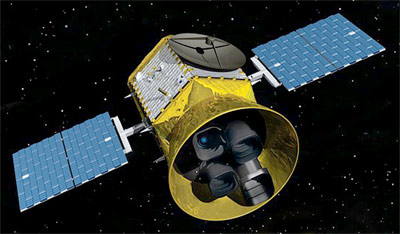
TESS has a group of four wide field cameras each with four large CCD imagers that will collect photometric data at a relatively high cadence, and therefore generate a ton of data.

enter image description here

above: "TESS (Astro-EX 1) [MIT]" From Gunter's Space Page.

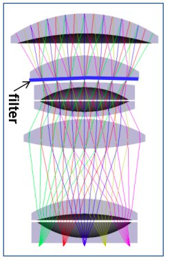
TESS' four cameras are based on lenses, and so unlike large telescopes with secondary mirrors suspended on "spider" mounts, I'm not aware of anything in the optical path that could cause a four-fold "star pattern" for bright stars.

enter image description here

The cameras do collect images with CCDs and so we can expect those artifacts.

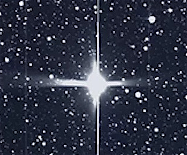
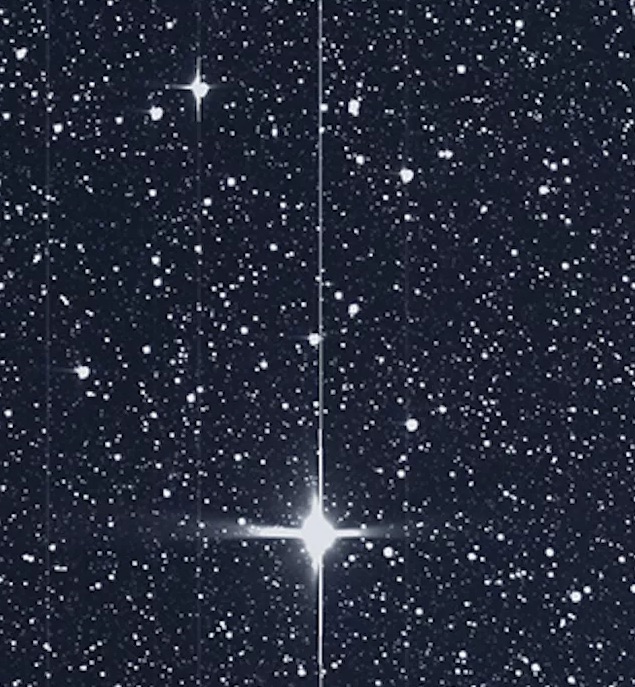
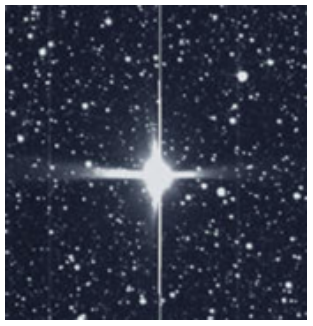
But when I look at the following images (top one is 2x and sharpened) from Axios' NASA's new planet-hunting spacecraft sends back first images it looks more like scattered light from an improperly cleaned lens, with some remaining horizontal and vertical streaks from a dirty shirt tail.

In fact one of the biggest advantages of using lens-based telescopes for deep-sky imaging is the minimization of scattered light. For example the Dragonfly Telescope described in the question What (actually) is the “deprojected half-light radius” of this almost-all-dark-matter Galaxy? (also Petapixel and U. Toronto)

Question: What is going on here? In addition to the long vertical line that I assume is a well-understood CCD artifact, there are four more fuzzy, diffuse, slightly curved lines. What is causing those?


See also NYTimes: NASA’s TESS Starts Collecting Planets

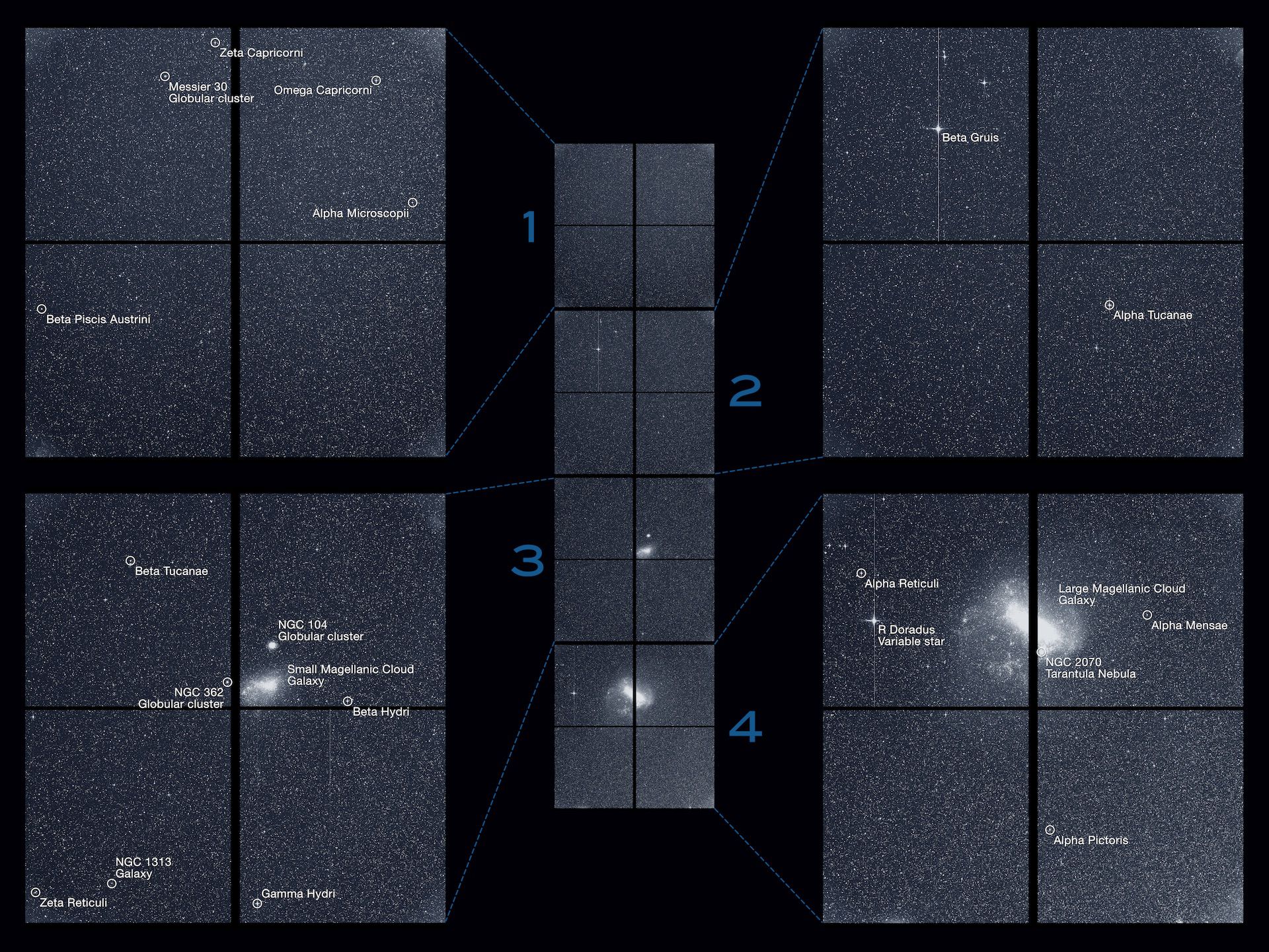
Images from Axios (of all places!):

below x2: "NASA's TESS spacecraft captured this swath of the southern sky in its “first light” science image on Aug. 7, 2018." Photo: NASA/MIT/TESS

TESS' first images

TESS' first images

below: "The TESS satellite captured this strip of stars and galaxies in the southern sky during one 30-minute period on Tuesday, Aug. 7. Notable features in this swath of the southern sky include the Large and Small Magellanic Clouds and a globular cluster called NGC 104, also known as 47 Tucanae." Credit: NASA/MIT/TESS.
TESS' first images

$\endgroup$
5
  • $\begingroup$ I haven't enough time for proper answer now, but. I suppose there are two different artifacts. The vertical lines are because of ccd saturation (you can google the term). The cross-like ones should be diffraction patterns I think. Reflector telescopes have features like this because of secodary mirror holding structure, but TESS have refractors, not reflectors. Maybe diafragma hole have square form. $\endgroup$
    – Heopps
    Commented Sep 18, 2018 at 11:24
  • $\begingroup$ @Heopps I don't see a square aperture in the design, what about a double reflection - off of the CCD face and the back again from a lens surface? Diffraction from the rectilinear CCD pattern would produce a cross, and a second reflection from a curved lens surface would cause it to be slightly curved (as these seem to be) iue.tuwien.ac.at/phd/minixhofer/node60.html $\endgroup$
    – uhoh
    Commented Sep 18, 2018 at 11:35
  • $\begingroup$ @uhoh If you don't ask this in Photo.SE I will ask one similar. This would be a very good question there as well. Let me know. $\endgroup$
    – Muze
    Commented Jan 5, 2019 at 1:37
  • $\begingroup$ @Muze I've mentioned this question in the chat room there, twice now. Last time I also mentioned the bounty. I originally decided to post here first and now that there is an answer I can't delete here and post there, and I won't double post. If you can think of a different but related question to ask there, go for it. $\endgroup$
    – uhoh
    Commented Jan 5, 2019 at 2:12
  • $\begingroup$ @uhoh what causes rays to come out of points of light? What is used to reduce that effect? $\endgroup$
    – Muze
    Commented Jan 5, 2019 at 4:26

2 Answers 2

5
$\begingroup$

The fuzzy light you mention are diffraction effects and the light baffles used are rectangular, which would give you the four-sided pattern. There is a paper that goes over the optical design where they also address the anticipated stray light effects (including back-reflections, known as ''ghost'' reflections). I don't know anything about this particular CCD, but the bright, vertical lines do look like they are what's known as ''blooming'' in CCDs, where there is so much charge due to a bright region that it gets dragged across the sensor as the charge is read out (for what it's worth, CMOS sensors don't have this particular problem, or it at least doesn't manifest itself like this).

$\endgroup$
3
  • 1
    $\begingroup$ Thanks for the reference! Wouldn't the external light baffles be placed outside of the optical path for rays that reach the CCD? Common sense and Figure 5 would suggest it, no? Can you find some discussion that adds credence to this large angle diffraction being caused by the baffles? It's just that I'm really surprised! $\endgroup$
    – uhoh
    Commented Sep 19, 2018 at 18:19
  • 2
    $\begingroup$ I'm just speculating, because that paper is rather terse, but they state that because their original design didn't have a field stop, they inserted an internal baffle between lenses 5 and 6, which they show in Figures 1, 2, and 4. However, they state that it was removed because it didn't cut down enough stray light to justify the extra size and weight. They might have designed the external baffles based on the internal baffle being there, so when they removed the internal one, then perhaps their external ones are now effectively acting as a field stop.. $\endgroup$
    – Dave
    Commented Sep 19, 2018 at 18:36
  • 1
    $\begingroup$ I think I've found it! space.stackexchange.com/a/35058/12102 $\endgroup$
    – uhoh
    Commented Mar 26, 2019 at 13:37
3
$\begingroup$

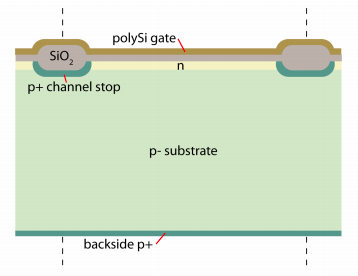
The artifacts described in the question are due to internal reflections within the silicon of the CCD chips. For TESS' long wavelength bandpass (red and near IR; 600 to 1000 nm) silicon is only weakly absorbing and light bounces around inside the thinned (~100 um) silicon substrate. The patterns of the polysilicon gates and associated X stop cause diffraction in X and Y, and since the light hitting the sensor is not always at normal incidence, the diffracted extensions can be curved.

enter image description here enter image description here

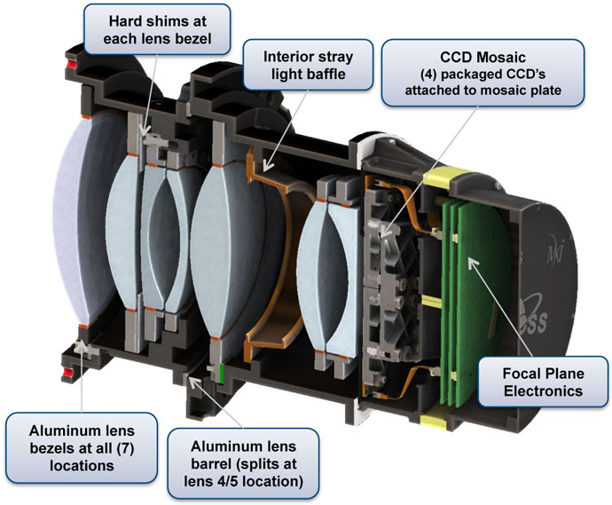
left: Reach-through Effect in Deep Depletion TESS CCDs "Figure 6. Cross section of the CCD array perpendicular to the direction of charge transfer, along the gate between two channel stops. right: Optical Design of the Camera for Transiting Exoplanet Survey Satellite (TESS)

Further reading:


From TESS Instrument Handbook Version 0.1 (Draft of 6 December 2018):

6.7 Image Saturation

A cursory glance at the image of a very saturated star (Figure 6.7) reveals several features:

  • The standard along-the-column charge bleed due to saturation
  • Diffuse image extensions in the column direction
  • Diffuse image extensions in the row direction

These effects, and others, are described below.

TESS image artifacts

Figure 6.7: This image of a saturated star in an FFI shows three primary features: the bloom of charge due to saturation, the extended horizontal feature that is due to reflection of red light within the CCD silicon bulk, and a smaller vertical structure, also due to light reflection within the silicon bulk.

6.7.1 Blooming

For bright stars the amount of charge generated by photons can exceed the full well capacity of a pixel, and electrons begin to spill over into adjacent pixels along the same column (the charge barrier in the CCD is much lower along the columns), this phenomenon is called ”blooming”. The spilled charge forms a bright thin vertical line in the image...

6.7.2 “Mustache”

Diffuse vertical and horizontal image extensions seen in some saturated images are due to reflections of long-wavelength light within the bulk silicon of the CCDs. Since the surface of silicon at that side is not flat, the reflections will go sideways, along the rows.

The channel-stop regions that serve to separate pixels in the horizontal (row) direction form vertical structures running along the surface: there, the Silicon - SiO2 interface is curved to form the channel-stop regions. When illuminated by light that travels perpendicular to the CCD surface, the side walls of channel stop regions partially reflect the light along the rows. If the star is near the center of the camera field of view, the reflected horizontal rays are very well aligned with rows. If the star location on the detector is far from the camera center, the incident light is not normal to the silicon surface. In this case, the reflections from the channel stops become tilted relative to the CCD rows, spreading into adjacent rows and creating a mustache-like shape. The direction of the tilt is opposite on the opposite sides of the field of view: the mustache curves away from the x-axis passing through the optic axis of the camera.

In addition to that, the mustache sidelobes become correspondingly asymmetrical when the star is shifted to the left or to the right from the center, which can be explained by the difference in reflection angles. As a result, the mustache lobe is longer in the direction away from the y-axis passing through the optic axis of the camera.

A similar phenomenon explains vertical lobes, which are slightly misaligned with the strictly vertical bloomed column, forming similar mustache in vertical direction, in addition to the cleanly vertical bloomed column. In this case deeply penetrating red component of incoming light is reflected from the edges of horizontally running structures formed by CCD polysilicon gates. As with the horizontal lobes, the deviation from completely vertical is caused by the fact that star light near the periphery of the field of view hits CCD surface from the direction that is not orthogonal to the surface.

A fuller explanation of the physics of the saturated images will be presented in Prigozhin (2019).

$\endgroup$

Your Answer

By clicking “Post Your Answer”, you agree to our terms of service and acknowledge you have read our privacy policy.

Not the answer you're looking for? Browse other questions tagged or ask your own question.